U.S. flag

An official website of the United States government

Here’s how you know

Dot gov

Official websites use .gov
A .gov website belongs to an official government organization in the United States.

HTTPS

Secure .gov websites use HTTPS
A lock (LockA locked padlock) or https:// means you have safely connected to the .gov website. Share sensitive information only on official, secure websites.

  • Environmental Topics
  • Laws & Regulations
  • Report a Violation
  • About EPA
Contact Us

Grantee Research Project Results

2011 Progress Report: Aptamer Capture and Optical Interferometric Detection of Cyanobacteria

EPA Grant Number: R833839
Title: Aptamer Capture and Optical Interferometric Detection of Cyanobacteria
Investigators: Campbell, Daniel P , Xu, Jie , Ellington, Andy
Current Investigators: Campbell, Daniel P , Ellington, Andy , Xu, Jie
Institution: Georgia Institute of Technology , The University of Texas at Austin
EPA Project Officer: Aja, Hayley
Project Period: June 1, 2008 through April 30, 2011 (Extended to January 31, 2013)
Project Period Covered by this Report: June 1, 2011 through May 31,2012
Project Amount: $600,000
RFA: Development and Evaluation of Innovative Approaches for the Quantitative Assessment of Pathogens and Cyanobacteria and Their Toxins in Drinking Water (2007) RFA Text |  Recipients Lists
Research Category: Drinking Water , Water

Objective:

Develop a sensor capable of detecting cyanobacterial toxins using aptamers as capture receptor.

Progress Summary:

The program was to develop aptamers, which are synthetic antibodies for cyanobacterial toxins, and bind them onto the Georgia Tech Research Institute’s planar waveguide interferometric sensor. The aptamer response is to be compared to the response obtained from natural antibodies. Of the three cyanobacterial toxins – anatoxin-a, cylindrospermopsin and microcystin-LR, shown in Figure 1 – the microcystin toxin, its antibody and aptamer are being investigated.
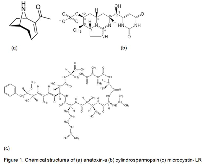
 
 
Figure 1
 

Aptamers and Antibodies

The antibodies for microcystin-LR were supplied by the Mohammed Zourob group in Montreal. In addition, some commercially available antibodies were obtained from EnviroLogix. EnviroLogix also supplied an experimental assay test kit for the detection and quantification of the toxin, if required. The aptamers for the microcystin-LR were developed and supplied by the Andy Ellington Group at the University of Texas in Austin. The aptamers were generated by the SELEX method. This method involves binding the target molecule, the toxin, to a solid support of a chromatographic column. A very large library of oligonucleotides is passed through the column where some of the oligomers bind with the toxin bound to the column. After passing the oligomers through the column, the column is washed to remove any materials that are not bound to the toxin. The aptamer/toxin complex is broken up and the aptamers are removed from the column. Additional aptamer material for microcystin-LR was synthesized by means of the polymerase chain reaction to produce enough material for the experiments. The microcystin-LR toxin was obtained from Cayman Chemical Company.
 
Waveguides
 
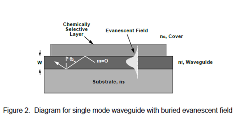
Planar waveguides are the critical element for the transducer used for the antibody/toxin and aptamer/toxin assay. Planar waveguides have evanescent fields sensitive to index of refraction changes in the volume immediately above the waveguide surface. These fields extend up to 5000 Å above the surface. Placing a chemically sensitive film, be it a polymer or a biorecognition layer, within this region provides the basis for a chem/bio sensor (Figure 2).
 
Figure 2
 
 
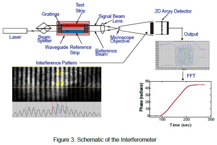
Chemical or physical interactions change the index of refraction, causing the propagating light speed, or phase, to change in a direction opposite to that of the index change. To measure this change a reference propagating beam, adjacent to the sensing beam, is optically combined with the sensing beam creating an interference pattern of alternating dark and light fringes (Figure 3). When chemical or physical changes occur in the sensing arm, the interference pattern will shift producing a sinusoidal output. With detectable sensitivities on the order of 0.01 radians index changes less than 10-6 can be measured. The sensing mechanism for the biosensor is active because it utilizes a molecular recognition element to bind with the targeted toxin and this binding causes a phase response in the interferometer.


Figure 3
 
 
Waveguide Fabrication
 
Waveguides are the critical element for the transducer used for the antibody/toxin and aptamer/toxin assay as well as all sensor projects being conducted here at GTRI. Waveguide fabrication has proven to be the most difficult challenge of this project. This should not be the case because the procedure for fabrication is very straightforward. The input and output gratings are rendered into the fused silica substrate by photolithography followed by reactive ion etching, which defines the grating pattern into the silica to a depth of 700 Å. The period of the grating is 720 nm. At that dimension one is near the diffraction limit of the light used in the photolithography. One may think this could be a cause for concern, but in the past the grating fabrication has gone quite smoothly. After the gratings are etched, the silicon oxynitride waveguide material is deposited by means of plasma enhanced chemical vapor deposition. The silicon oxynitride is deposited to a thickness of approximately 1500 Å and a refractive index of approximately 1.85. The high index is what confines the optical beam in the waveguide layer as well as generates the evanescent field that does the sensing. After the waveguide material is deposited, another photolithography step is used to define the channels of the interferometer. The channels are defined with photoresist and in the area not defined by the photoresist is deposited 5-6000 Å of silicon dioxide, which is enough material to bury the evanescent field in regions not used for sensing.
 
Over the past 4 years less than a handful of waveguides have been produced for all projects in the lab. The facility that is used for fabricating waveguides is a facility that is used by students to fabricate various electronic devices. With a wide range of people using the Microelectronics Research Center (MIRC), for it is a teaching facility and not designed for high throughput fabrication, keeping this equipment up and functioning at its best provides quite a challenge, for there is a tendency for the equipment to be overused and therefore likely to break down with little incentive to repair it in short order. This equipment is out of the hands for GTRI and we are at the mercy of the Microelectronic Center to repair and keep the equipment functioning properly.
 
After the waveguide material is deposited, photoresist is again spun on the substrate and a pattern is defined for the channels that define the path length of the interferometer. An IAD, ion-assisted deposition, is used to deposit a 5-6000 Å layer of silicon dioxide over the entire substrate except where the photoresist define the sensing and reference channels. During the past 4 years the IAD system has had its share of problems when it comes to depositing good quality films of silicon dioxide.
 
Funding for fabrication was pretty much exhausted without fabricating any quality waveguides. In mid-2012, equipment at MIRC was working and waveguides for various projects finally were produced although the yield was still quite low. To achieve a useable number of waveguides in the MIRC system, 4-inch substrates were used, which allows for the manufacture of 16 waveguides on one substrate. Having 16 waveguides produced for each substrate increased the probability that useable waveguides would be fabricated. This was the case but the size of the fabricated waveguides was not the size needed for the toxin experiment but slightly smaller. Reconstructing the sensor head was necessary to properly fit the new waveguides. The reason that these waveguides were of smaller size is that they were not fabricated for GTRI but for Lumense, a startup company, founded to commercialize the sensor. Lumense’s sensor head holds a smaller waveguide that the sensor head used at GTRI. In the meantime, a lab-wide search for useable waveguides was conducted. This search scoured the lab for waveguides that then were cleaned followed by evaluation of the coupling angle and the propagation of light in each of the waveguides. Of the several score waveguides cleaned and examined only a few working waveguides were located.
 
Of the waveguides found during the waveguide search, only two good quality waveguides were found of the biosensor design, a design in which both arms of the interferometer are exposed. A few more of the buried reference waveguides were found in which, as the name implies, only one channel is open and the other has the thick silicon dioxide deposited. A buried reference waveguide is typically not used for biosensor experiments but can be used in a pinch if there are not many other influences that would produce a response other than the desired molecular recognition element binding to the targeted toxin. Other events that can produce a response include temperature differences between the buried channel and the sensing channel. Also bulk refractive index changes in the solution would produce a response without a binding event. This response is typically due to the changing of buffers between the establishing of a baseline and the composition of the test solution. These two interferents can be minimized but they do decrease the ultimate sensitivity of the waveguide.
 
Waveguides are being made with either a single interferometer or four interferometers on a single chip. The spacing of the two channels is only 100 microns between the sensing and reference channels. Spacing between adjacent interferometers in the four interferometer design is 1.5 mm. The design of the four interferometer chip is shown in Figure 4. Two different designs for the input grating have the grating continuously illuminating the entire chip or segmented (not shown) to light up only the channels comprising the interferometer. The output gratings are smaller than the channel width so as to capture light that only propagates down the middle of the channel. In addition, the doublets of output gratings are staggered in the propagation direction so as to image the interference patterns on the camera detector without overlap of adjacent interferometric fringes.
 
Waveguide Patterning
 
Photomasks were generated for both steps of the waveguide fabrication – the gratings masks and the channel masks. Masks were made for both the single interferometer chip and the four interferometer multiplexed chip. These masks were fabricated at the onset of the program. Another mask recently was generated that will define the chemistry used for sensing and possibly the reference channels. These channel patterns are 10 microns larger on the dimensions between adjacent channels – sensing and reference. The chemistry mask, as it is called, leaves photoresist on the sensing and reference channels so that a fluorosilane can be deposited in the area around the channels, making the waveguide unwettable everywhere except the sensing and reference channels. Tridecafluoro-1,1,2,2-tetrahydrooctyl-1-dichlorosilane was initially used to covalently attach the fluorosilane to the silicon dioxide, rendering the non-channel areas unwettable. Contact angles were greater than 90 degrees indicating that the surface had been fluorinated. However, it was found out that the difunctional silane, i.e., the dichloro silane, did not produce as extreme of an unwettable surface as required to prevent the aqueous chemistry to remain within the channels. This problem was resolved by using a trifunctional silane, tridecafluoro-1,1,2,2-tetrahydrooctyl-1-trichlorosilane. This silane gave a contact angle of greater than 110 degrees, which indicates that the hydrophobicity is greater with the trifunctional silane than the difunctional silane. One disadvantage of the trifunctional silane is that it leaves a somewhat cloudy deposit on the waveguide. It takes a bit of work to wipe the cloudy layer off with methanol.
 
Attachment of the aptamers to the waveguide surface can be accomplished in a number of ways, both covalently and electrostatically. Traditionally, covalent attachment is used to attach the receptor molecule to the surface. It also is the method specified in the original proposal. However, there is a difficulty with the quality of the waveguide in that the amount of light propagating down the waveguide is not adequate for the covalent attachment of the sensing film. The method of attachment tried was to take 3-glycidoxypropyldimethylchlorosilane and have it react with the surface hydroxyls on the waveguide channel surface. The epoxide ring of the 3-glycidoxypropyldimethylsilanyl group is opened and oxidized with sodium periodate in 80% acetic acid to form the aldehyde. A protein then can be attached via reductive amination with sodium cyanoborohydride. This protein can be either a biotinylated bovine serum albumin or avidin. A biotinylated aptamer then is bound to the protein, either directly to the avidin or to the avidin that was first bound to the albumin. When this scheme was tried, the resulting albumin-derivatized waveguide would no longer guide light. The poor quality of the waveguide is thought to be the problem. In addition, these steps are done without the chip set up in the sensor head where the waveguide can dry out between steps.
 
An electrostatic method provides an alternative to the covalent attachment in which all the steps can be done with the waveguide chip set up in the device and the waveguide never being allowed to dry out between steps. Two approaches can be used here and the first one appears to work well. Biotinylated bovine serum albumin is electrostatically bound from solution and it can be monitored with the transducer to determine the amount of binding or chemical change. The next step is to couple avidin to the surface through the avidin/biotin complex formation, a very strong complex. And finally a biotinylated aptamer completes the functionalization of the waveguide. A similar process was tried with a biotinylated RNA and each step worked and was able to be monitored with the transducer through each step in the process. It is also possible that avidin itself can be electrostatically bound to the surface followed by the biotinylated aptamer to form the derivatized surface. To utilize these schemes one has to use the buried reference waveguide in order to form the differential between the sensing arm and the reference arm. The advantage is that each step can be monitored along the way, in addition to the final toxin assay.
 
The biggest disadvantage of using the buried reference approach to produce the derivatized surface is that any temperature difference between the baseline solution and the assay solution will produce a response, although this response is typically quite small. It can be minimized by using solutions at the same temperature. This method is currently being used to assess the interferometric transducer’s ability to detect and quantify the microcystin-LR toxin.
 
Sensor Head
All during the project, the sensor head, which holds the laser, waveguide and camera detector, has been improved. The initial devices were machined from a piece of delrin. A cheaper and simpler method for producing the sensor head was found by using rapid prototyping of the sensor head. A company called Quick Parts in Atlanta fabricated the new sensor heads which uses a process that fuses together small beads of polymer into the shape desired. The sensor head is fabricated from Duroform, a type of nylon.
 
Software
Software to take the raw interferometric signal and convert it to total phase shift for each interferometer using real-time fast Fourier transform is ready and waiting to be applied. The details of the software will be in the final report. The latest software design examines the fringe pattern and finds the best region of interest automatically, without human intervention. Currently, one still has to visually interpret the region of the fringe pattern that looks the best.


Future Activities:

The future activities are to: biotinylate the aptamers, bind the aptamers to the waveguide surface, and test with microcystin.

Supplemental Keywords:

Interferometric sensor, microcystin, waveguide, RFA, Scientific Discipline, INTERNATIONAL COOPERATION, Water, Health Risk Assessment, Environmental Chemistry, Drinking Water, Environmental Engineering, Environmental Monitoring, microbial contamination, gene microarray assay, early warning, microbial risk assessment, monitoring, aquatic organisms, drinking water system, drinking water contaminants, other - risk assessment, cyanobacteria

Progress and Final Reports:

Original Abstract
  • 2008
  • 2009 Progress Report
  • 2010
  • Final Report
  • Top of Page

    The perspectives, information and conclusions conveyed in research project abstracts, progress reports, final reports, journal abstracts and journal publications convey the viewpoints of the principal investigator and may not represent the views and policies of ORD and EPA. Conclusions drawn by the principal investigators have not been reviewed by the Agency.

    Project Research Results

    • Final Report
    • 2010
    • 2009 Progress Report
    • 2008
    • Original Abstract

    Site Navigation

    • Grantee Research Project Results Home
    • Grantee Research Project Results Basic Search
    • Grantee Research Project Results Advanced Search
    • Grantee Research Project Results Fielded Search
    • Publication search
    • EPA Regional Search

    Related Information

    • Search Help
    • About our data collection
    • Research Grants
    • P3: Student Design Competition
    • Research Fellowships
    • Small Business Innovation Research (SBIR)
    Contact Us to ask a question, provide feedback, or report a problem.
    Last updated April 28, 2023
    United States Environmental Protection Agency

    Discover.

    • Accessibility
    • Budget & Performance
    • Contracting
    • EPA www Web Snapshot
    • Grants
    • No FEAR Act Data
    • Plain Writing
    • Privacy
    • Privacy and Security Notice

    Connect.

    • Data.gov
    • Inspector General
    • Jobs
    • Newsroom
    • Open Government
    • Regulations.gov
    • Subscribe
    • USA.gov
    • White House

    Ask.

    • Contact EPA
    • EPA Disclaimers
    • Hotlines
    • FOIA Requests
    • Frequent Questions

    Follow.