
Grantee Research Project Results
Final Report: Comparative Life Cycle Analysis of Nano- and Bulk-materials in Photovoltaic Energy Generation
EPA Grant Number: R833334Title: Comparative Life Cycle Analysis of Nano- and Bulk-materials in Photovoltaic Energy Generation
Investigators: Fthenakis, Vasilis , Themelis, Nickolas J.
Institution: Columbia University in the City of New York
EPA Project Officer: Hahn, Intaek
Project Period: June 1, 2007 through May 31, 2009
Project Amount: $200,000
RFA: Exploratory Research: Nanotechnology Research Grants Investigating Environmental and Human Health Effects of Manufactured Nanomaterials: a Joint Research Solicitation-EPA, NSF, NIOSH, NIEHS (2006) RFA Text | Recipients Lists
Research Category: Nanotechnology , Safer Chemicals
Objective:
We examined the energy and material requirements during the life cycles of representative nanotechnology applications in photovoltaic (PV) devices, along with associated hazards, and compared them with the material- and energy flows and hazards in the technologies that they may replace. We evaluated two systems of nanotechnology, one in R&D and the other in the early stages of commercial development: viz., nano-rod based CdTe PV and amorphous silicon (a-Si) muti-junction PVs with nano-crystalline silicon (nc-Si) bottom layer. Because they currently are not produced on a commercial scale, actual life cycle flows of material, energy, and emissions are unavailable. We formulated the life cycle energy and emissions for these technologies based on the following parameters: 1) amounts of materials required in the whole PV system; 2) material utilization rates/process efficiencies; 3) deposition process rates; and, 4) system electric-conversion efficiency. Current and prospective designs were analyzed and compared in terms of life cycle energy and emissions.Summary/Accomplishments (Outputs/Outcomes):
The nano CdTe PV process evaluated in this project uses nano CdTe and nano CdSe rods that are sequentially spin casted from solution to create an all inorganic ultrathin donor-acceptor solar cell. As nano CdTe/CdSe solar cell technology is still in very early stages of development, energy, materials and emission data from commercial production lines are unavailable. Escalating factors were defined to predict the material utilization of the nano CdTe/CdSe in a commercial process, as the ratio between lab scale amount and that projected in a commercial production line. For cell materials (i.e. CdO, Te and Se) a scaling factor of 100 was found to represent the difference in the efficiencies between lab scale and commercial scale film formation. Material usage (g/m2), when only cell materials are included (i.e. CdTe, CdS and other Cd compounds for the micro process and CdO, Se and Te for the nano process), is around 51.4 g/m2 for the micro process and 14.9 g/m2 for the projected commercial nano process. However, if all the other reactants are included, the material requirements for the projected commercial nano process escalate to 6.5 kg/m2, 0.6 kg/m2, and 0.06 kg/m2 for each scenario evaluated. The primary energy of the nano CdTe/CdSe PV process is 47,600 MJp/m2 at the lab level, mostly from cell materials and reactants usage, with solvents accounting for 86% of the total. If only cell materials are taken into account, the nano CdTe/CdSe PV process has a primary energy value of 46.9 MJp/m2 at the lab level and 0.47MJp/m2 at the projected commercial level, while the micro process requires 27.3 MJ/m2. The solvents and phosphorus compounds used in growing and purifying the nanoparticles dominate the primary energy use (Figure 1). Commercial producers might adopt recycling or energy recovery of the used solvents, which could further lower energy use.
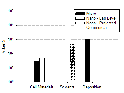
Figure 1: Cradle-to-gate demands of primary energy of the micro- and nano- CdTe techniques.
Our investigation of future nanostructure based a-Si PV modules involved a comparison between a triple junction a-Si module, a-Si/a-SiGe/a-SiGe, and three prospective combinations of hybrid amorphous- and crystalline-silicon cells being developed by United Solar. The first configuration is a tandem junction that consists of a-Si top layer and nc-Si bottom layer, i.e., a-Si/nc-Si; the second configuration is a triple junction with nc-Si as the bottom layer, i.e., a-Si/a-SiGe/nc-Si; and, lastly, a triple junction with two layers of nc-Si, i.e., a-Si/nc-Si/nc-Si.
The energy pay-back times (EPBTs) of the new designs, with nc-Si as a bottom layer for the reference cases, are found to be significantly longer (i.e.15-30%) than those of the current triple-junction a-Si module, viz., 0.8 year. This result is primarily attributed to the higher primary energy requirement of the new design. Moreover, the efficiencies of the new designs are no higher than those of the current triple junction. We note that our estimates of the EPBTs for the new designs are unrealistic; with such low module efficiency, they will not be commercialized. With an EPBT of <1 year under the average U.S. conditions, all of these new designs exhibit potential advantages over bulk Si PVs whose EPBT is 1.2-1.7 years under the same condition. Figure 2 gives the EPBTs of the future scenarios with reduced primary energy demand based on advanced deposition processes. The expected gains in module efficiency if coupled with a high rate of deposition and lower gas usages could reduce dramatically the EPBTs. For example, using the anticipated future efficiency of 10% for a-Si/nc-Si, the average EPBT corresponds to ~0.5 year for all designs.
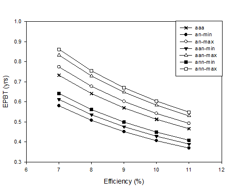
Figure 2: EPBT of future multi-junction a-Si module designs plotted over stabilized conversion efficiency under the average U.S. insolation, 1800 kWh/m2/yr and a performance ratio of 0.75. “aaa, an, aan, and ann”, respectively, corresponds to a-Si/a-SiGe/a-SiGe, a-Si/nc-Si, a-Si/a-SiGe/nc-Si, and a-Si/nc-Si/nc-Si.
Conclusions:
Several critical conclusions have been derived to improve the sustainability of the current nano-technology-based CdTe photovoltaic technology. First, the process needs to be scaled up to reduce the amount of solvent used in purifying nano particles. Second, nano-CdTe particles need to be deposited through ink-jet printing method to minimize material loss and energy demand instead of the current lab-scale spin casting. Finally, recycling or energy recovery will be critical to abate the environmental impact from those solvents and precursors used during the synthesis of nano-CdTe powder.
Our analysis of nano-structured based a-Si PV modules show that for these technologies significant progress is needed in the production and conversion efficiencies to pass the sustainability performances of their micro-based counterparts. It is obvious, however, that commercial versions of these technologies will have much improved parameters since those efficiencies are also crucial barometers for surviving fierce competition in the PV market. According to future scenarios with a projected efficiency of 10% and deposition rate of 2-3 nm/s, the EPBTs could further drop by ~30% from the above scenario. Besides PECVD, other film-deposition technologies might produce nc-Si at an even higher rate, although the deposition quality is not satisfactory yet. A timely update of this analysis will be needed in the future if these new technologies dominate.
Journal Articles on this Report : 1 Displayed | Download in RIS Format
| Other project views: | All 6 publications | 1 publications in selected types | All 1 journal articles |
|---|
| Type | Citation | ||
|---|---|---|---|
|
|
Kim HC, Fthenakis VM. Comparative life-cycle energy payback analysis of multi-junction a-SiGe and nanocrystalline/a-Si modules. Progress In Photovoltaics 2011;19(2):228-239. |
R833334 (Final) |
Exit |
Supplemental Keywords:
cadmium telluride (CdTe), inkjet printing, amorphous silicon (a-Si), nano-crystalline silicon (nc-Si), primary energy, energy payback timeProgress and Final Reports:
Original AbstractThe perspectives, information and conclusions conveyed in research project abstracts, progress reports, final reports, journal abstracts and journal publications convey the viewpoints of the principal investigator and may not represent the views and policies of ORD and EPA. Conclusions drawn by the principal investigators have not been reviewed by the Agency.